The topography or elemental composition of sample surfaces can be determined using scanning electron microscopy (SEM) in conjunction with energy-dispersive X-ray spectroscopy (EDX). The elemental composition can be measured quantitatively and with spatial resolution. A microscope from JEOL (JSM 7610F) with an EDX detector (EDAX, AMETEC Element 4.) is used here.
The SEM is equipped with the following detectors:
- SE-Outlens detector type Everhart-Thornley (secondary electrons; topography contrast due to shadowing effects; working distance 10 mm; magnification 25-5,000 x)
- SE-Inlens detector (secondary electrons; material contrast; working distance 10mm, magnification 500-1,000,000 x, resolution max. 1nm)
- BSE outlens detector (backscattered electrons; material contrast; working distance 8 mm; flat surfaces; resolution max. 3 nm)
In addition, a STEM (Scanning Transmission Electron Microscopy) detector is available for thin samples, where measurements are made in transmission. The samples for the SEM should be vacuum-stable and conductive. Non-conductive samples can be sputtered with very thin metal films (gold, platinum) and can therefore also be measured.
Contact person: Dipl-Ing. Silvia Löffelholz
Measurement methods:
- Photoelectron spectroscopy (XPS, UPS)
- Auger electron spectroscopy (AES)
- Scanning tunneling microscopy (STM)
- Atomic force microscopy (AFM)
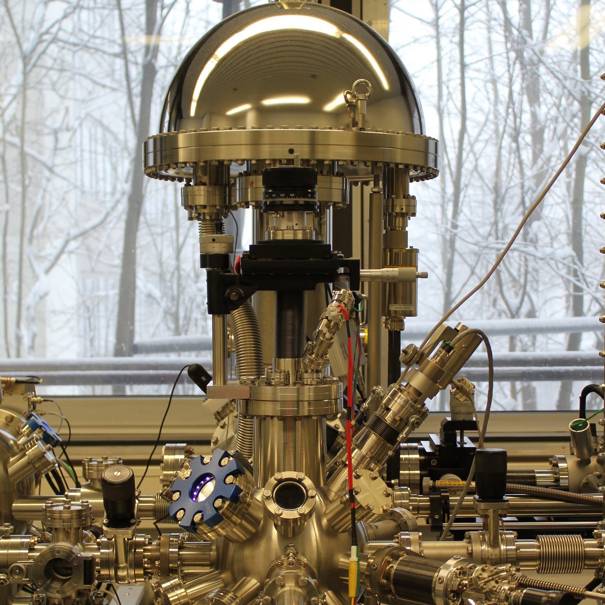
The Omicron UHV Nanoprobe System offers a wide range of possibilities for surface analysis and preparation. The high-vacuum system enables both targeted annealing and sputtering of the sample to prepare the sample surface. For special applications, organo and metal evaporators enable the evaporation of thin layers. The sample surface can be analyzed both in terms of chemical composition using spectroscopic methods (XPS, UPS, AES) and in terms of topographical properties using microscopic methods such as AFM and STM. The combination of spectroscopic methods in particular opens up a wide range of possible applications for the detailed structural elucidation of solid samples.
Measuring methods:
- X-ray photoelectron spectroscopy (XPS)
- Scanning tunneling microscopy (STM)
- Scanning atomic force microscopy (AFM)
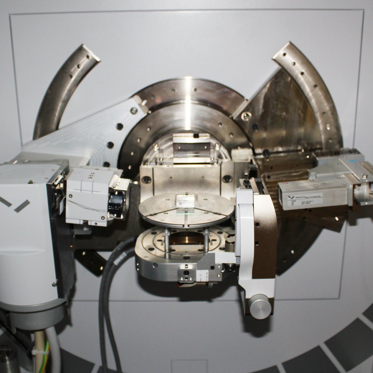
With the help of the Specs UHV-XPS/SPM system, samples can be analyzed both in terms of their chemical composition (XPS) and their topographical surface properties (STM/AFM). A special feature is the use of monochromatic X-rays, which are used for high-resolution chemical analysis of the sample surface. The preparative processes used include tempering and sputtering. The facility also has two PVD devices that can be used to prepare either molecular or metallic layers. For XPS and STM examinations, semiconducting as well as conductive materials can be used. The atomic force microscope (AFM) also allows the microscopic examination of non-conductive samples.
X-ray diffraction (XRD) can be used to analyze the crystallinity of samples (powders, solids, thin films). In addition, a quantitative analysis of phase composition is possible and databases are available to make statements about the composition of unknown crystalline samples. Furthermore, the average crystallite size of crystallites ≤ 0.1 μm can be determined using Scherrer's equation. A diffractometer from PANalytical Empyrean is available for XRD, which works with monochromatic CuKα radiation.
Raman and infrared (IR) vibrational spectroscopy is a non-contact analysis method for material characterization. A solid or liquid sample is irradiated with light in order to generate molecular movements. The resulting interactions then allow conclusions to be drawn about the properties of the sample. In general, Raman spectroscopy is based on the inelastic scattering of light when matter is irradiated by a monochromatic light source. In infrared spectroscopy, molecular vibrations are generated by absorption of light in the infrared region of the electromagnetic spectrum. These interactions are characteristic of the different chemical bonding conditions in a material. The resulting Raman and IR spectra serve as a "molecular fingerprint" and can be used to characterize unknown organic and inorganic samples.
Our working group has the following equipment at its disposal:
- VERTEX 70 V, RAM II-Raman modules with Ge detector (Nd:YAG 1064 nm laser) and ATR (A225/Q) (Bruker Optic GmbH)
With the VHX-1000 digital microscope from Keyence, sample surfaces can be imaged microscopically in reflected light geometry (incl. image composition function). The microscope also allows observation at different angles and the measurement of 3D structures within the resolution range. Two objectives (20x-200x; 100x-1000x) are available so that a larger magnification range is accessible.
Device: Keyence VK-X210
Measuring methods:
- Confocal Laser Scanning Microscopy (CLSM)
- Light microscopy
The good lateral resolution (approx. 160 nm) enables detailed images of many samples. On the software side, many images can be combined into one large image, so that large areas of the sample can be imaged even at high magnification. As the topography of the sample is recorded, it is possible to carry out roughness analyses or profile sections. Objects with low opacity in the wavelength range of the laser used for detection (408 nm) can be irradiated so that boundary layers or films can also be imaged. Due to different reflectivities in relation to the laser wavelength, material contrasts can sometimes be recognized. A wide-field microscopy image is also recorded.
In UV-Vis spectroscopy, the interaction of samples (solid or liquid in our case) with ultraviolet (UV) and visible (VIS) light is investigated. Two UV-Vis spectrophotometers are available for this purpose - the Cary 60 (wavelength range: 190 - 1100 nm) and the Cary 5000 (wavelength range: 175 - 3300 nm).
Both spectrometers can be used to measure both transmission and reflection. Liquids are generally measured in transmission.
The Cary 5000 can be used to measure in reflection with variable angles of incidence (20° to 70°, 0.5° steps). Measurements under electrochemical control (UV-Vis spectroelectrochemistry) are also possible. The Cary 60 also has connection options for fiber optics.
Our working group has two scanning tunneling microscopes (STM) and two atomic force microscopes (AFM). The STM records the electrical tunneling current that flows between a metallic tip and a conductive substrate, which are brought very close together but not in direct contact. In contrast to STM, AFM measures the electrostatic forces between the tip and the surface; it is therefore essential that the sample is non-conductive.
STM and AFM can also be used to study surface properties at the atomic level. Tunneling current or force can also be measured as a function of the distance between the tip and the surface of the sample, which can provide information about tip-sample interactions. Force-distance curves recorded by AFM can provide information about the structure of the electrolyte/solid interface.
We use the following devices:
- Two PicoScan 2500 STM (Molecular Imaging) controllers with in-house developed STM heads and scanners
- Two 5500 AFM systems from Keysight Technologies including AFM head (N9411A) and multipurpose scanners (N9520, type A or B)
We currently have 7 glove boxes from VAC, each of which is used for specific applications:
- Special design with connection to the ultra-high vacuum system; sample preparation takes place in the absence of oxygen, samples can be introduced directly
- Drying of sensitive samples and ionic liquids, electrochemical separation
- Testing battery material under inert gas
- Ultrapurebox for precise sample preparation under argon
- Electrochemical deposition and experiments with argon plasma
- Glovebox with integrated AFM device, can be operated from 2 sides / 2 persons
- Glovebox with integrated anti-vibration table to avoid vibrations during sensitive experiments
Contact person: N.N.